In this note, we are going to know about 8051 Microcontroller Pin Diagram and Function of Each Pin of the 8051 Microcontroller. Welcome to Poly Notes Hub, a leading destination for engineering notes for diploma and degree engineering students.
Author Name: Arun Paul.
What is 8051 Microcontroller?
The 8051 microcontroller is a popular 8-bit microcontroller designed by Intel in 1980. It is part of the MCS-51 family and is well-known for its simplicity, adaptability, and wide application in embedded systems. The 8051 microcontroller is widely used in industrial, commercial, and consumer applications including home appliances, automation systems, and robots.
The 8051 microcontroller is one of the most often used microcontrollers in embedded systems. It was designed by Intel and has since become an industry standard due to its basic architecture and flexibility. One of the most important aspects of working with the 8051 is understanding its pin diagram, which governs how the microcontroller interfaces with the outside world.

Key Features of 8051 Microcontroller
Before the discussion of the 8051 Microcontroller pin diagram, we have to know about some key features of the 8051 microcontroller.
- 8-bit CPU (processes 8-bit data at a time).
- Harvard architecture (separate memory spaces for program code and data).
- CISC (Complex Instruction Set Computer) design.
- 4 KB of on-chip program ROM (can vary in different variants).
- 128 bytes of on-chip data RAM.
- External memory support for program and data (up to 64 KB).
- 4 parallel I/O ports (P0, P1, P2, P3), each 8-bit wide.
- Uses an external crystal oscillator (typically 12 MHz) to generate clock signals.
8051 Microcontroller Pin Diagram
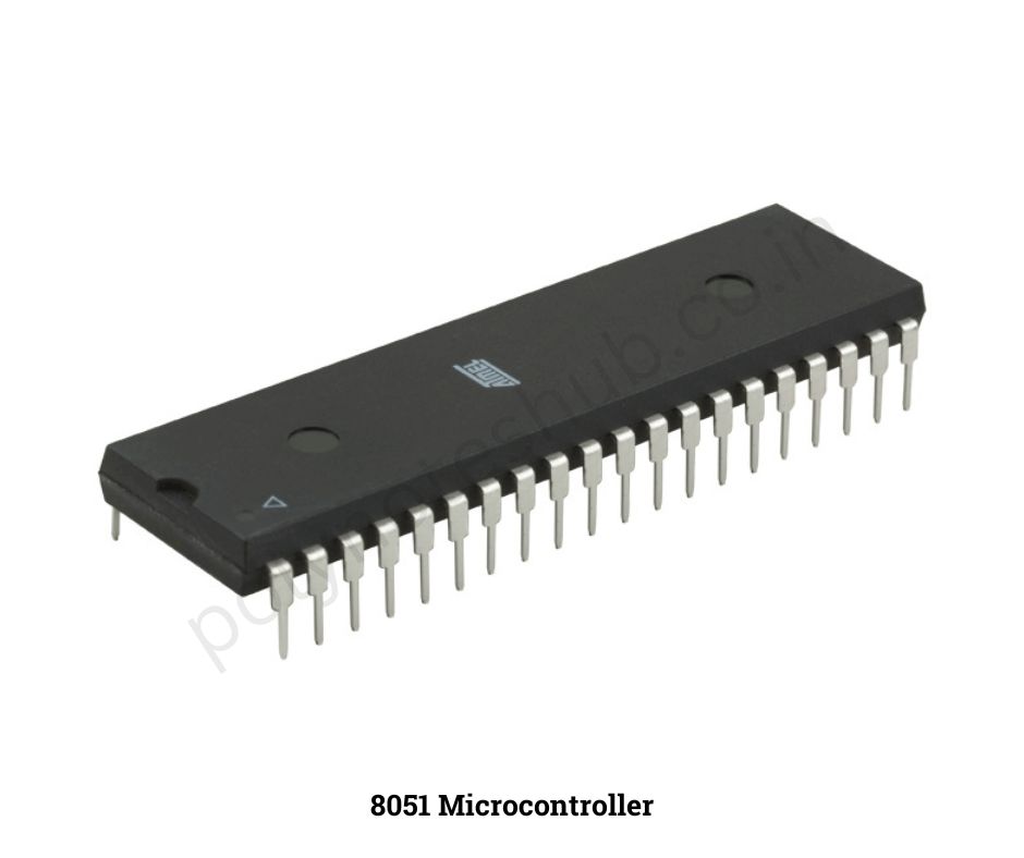
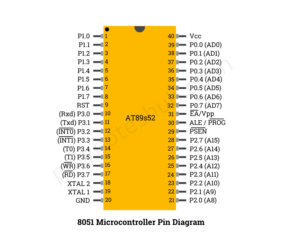
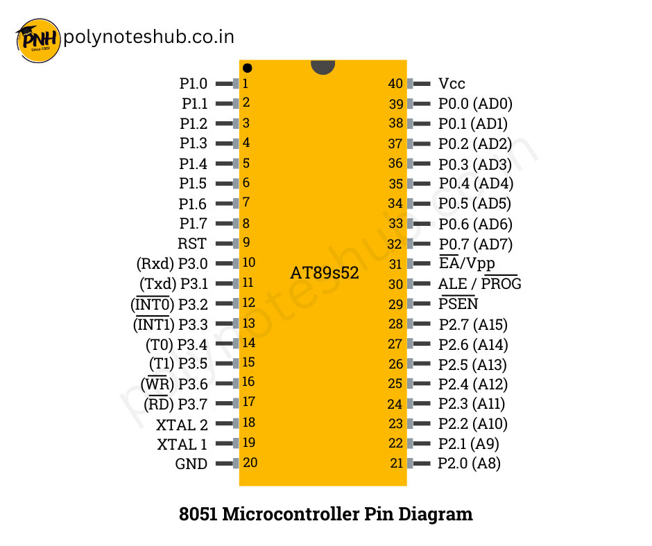
The 8051 microcontroller has a 40 pin Dual Inline Package (DIP). Each of these pins serves a distinct purpose, and understanding them is critical for developing projects and circuits using the 8051.
Let’s look at the pin diagram of 8051 Microcontroller and figure out what each group of pins is for.

I/O Ports (Input or Output Pins)
There are 32 input or output pins in total, divided into 4 ports:
- Port 0 (Pins 32 to 39): This port is open-drain and can be used for both I/O and external memory interfacing. When used for memory access, it carries the lower byte of address/data.
- Port 1 (Pins 1 to 8): This is a general-purpose I/O port.
- Port 2 (Pins 21 to 28): Also used for I/O. When external memory is accessed, it carries the higher order address.
- Port 3 (Pins 10 to 17): These pins serve dual functions. Besides I/O, they support special functions like interrupts, serial communication, and control signals.
Control Signals
- ALE (Pin 30): Stands for Address Latch Enable. This pin is used to de-multiplex the address/data signals from Port 0.
- PSEN (Pin 29): Program Store Enable – it is used to read external program memory.
- EA (Pin 31): External Access – When low, the microcontroller accesses code from external memory.
These control signals are critical in managing external memory interfacing and determining whether data is being fetched from internal or external ROM.
Power Supply and Reset Pin
- Vcc (Pin 40): Connected to the power supply to the circuit, usually +5V.
- GND (Pin 20): Ground reference.
- Reset Pin (Pin 9): This pin is used to reset the microcontroller. When a high pulse is given to this pin, it reinitializes the 8051 to its default state.
Timers and Counters
The 8051 has two timers, known as Timer 0 and Timer 1. These are programmed with special function registers and are used to generate time delays or count external events. These timer counter characteristics are particularly useful for real-time tasks.
Serial Communication
The 8051 supports serial communication via the TXD and RXD pins (part of Port 3). This function facilitates connectivity with other microcontrollers, computers, or serial devices, making the 8051 extremely versatile.
Internal RAM and ROM
- The 8051 contains 128 bytes of internal RAM for data storage.
- It has 4KB of ROM for storing the program code. However, external ROM can also be interfaced using Port 0, Port 2, and control pins like PSEN.
📌 Here is the short notes and function of each pin of this microcontroller –
- VCC (Pin 40): Supply voltage input (+5V) for the microcontroller.
- GND (Pin 20 and 40): Ground reference for the microcontroller.
- P0.x (Pin 32-39): General-purpose bidirectional I/O pins of Port 0.
- P1.x (Pin 1-8): General-purpose bidirectional I/O pins of Port 1.
- P2.x (Pin 21-28): General-purpose bidirectional I/O pins of Port 2.
- P3.x (Pin 10-17): General-purpose bidirectional I/O pins of Port 3.
- RST (Pin 9): External reset input. A low pulse on this pin resets the microcontroller.
- ALE/PROG (Pin 30): Address Latch Enable (ALE) and Program Pulse Input. Used to demultiplex the address and data during external memory access.
- PSEN (Pin 29): Program Store Enable. Used to enable external ROM memory.
- EA/VPP (Pin 31): External Access Enable (EA) and programming supply voltage (VPP) during EPROM programming.
- XTAL1 (Pin 19): Input for connecting an external crystal oscillator or resonator.
- XTAL2 (Pin 18): Output of the crystal oscillator or resonator.
- RD (Pin 39): Read control signal for external memory.
- WR (Pin 37): Write control signal for external memory.
- T0 (Pin 18): Timer 0 external input.
- T1 (Pin 17): Timer 1 external input.
- INT0 (Pin 12): External interrupt 0 input.
- INT1 (Pin 13): External interrupt 1 input.
- TXD (Pin 10): Serial transmission data.
- RXD (Pin 11): Serial reception data.
- T2EX (Pin 1): Timer 2 external count input.
- T2 (Pin 2): Timer 2 output/input.
- EX0 (Pin 3): External interrupt 0 enable input.
- EX1 (Pin 4): External interrupt 1 enable input.
- VCC (Pin 20): Supply voltage input (+5V) for the microcontroller.
These pins provide various functionalities, including general-purpose I/O, timers/counters, interrupt inputs, serial communication, external memory interfacing, and more. It’s important to consult the specific datasheet for your 8051 variant to get detailed information about each pin’s electrical characteristics and recommended usage.
The Pin Diagram of 8051 Microcontroller is an essential resource for understanding the architecture and functions of this popular microcontroller. It shows a graphic representation of the pin configuration, including the purpose and function of each pin. The 8051 Microcontroller Pin Diagram shows 40 pins organized into ports, power supply, clock, and control signals. For example, pins P0 to P3 act as input/output ports, while Vcc and GND provide power.
Conclusion
If you’re dealing with microcontroller-based circuits, you’ll need to understand the pin diagram of 8051 Microcontroller. Knowing what each pin accomplishes, from I/O ports to control signals, timers, serial communication, and how it it connected to the power supply, will help you build and debug your system more efficiently. Whether you’re utilizing the 8051 for academic projects or professional embedded applications, understanding its pin configuration is the first step toward success.


