In this note, we are going to know about the Block Diagram of 8051 Microcontroller. Welcome to Poly Notes Hub, a leading destination for engineering notes for diploma and degree engineering student.
Author Name: Arun Paul.
What is 8051 Microcontroller?
The 8051 microcontroller is a popular 8-bit microcontroller designed by Intel in 1980. It is part of the MCS-51 family and is well-known for its simplicity, adaptability, and wide application in embedded systems. The 8051 microcontroller is widely used in industrial, commercial, and consumer applications including home appliances, automation systems, and robots.

Key Features of 8051 Microcontroller
Before the discussion of the block diagram of 8051 microcontroller, we have to know about some key features of the 8051 microcontroller.
- 8-bit CPU (processes 8-bit data at a time).
- Harvard architecture (separate memory spaces for program code and data).
- CISC (Complex Instruction Set Computer) design.
- 4 KB of on-chip program ROM (can vary in different variants).
- 128 bytes of on-chip data RAM.
- External memory support for program and data (up to 64 KB).
- 4 parallel I/O ports (P0, P1, P2, P3), each 8-bit wide.
- Uses an external crystal oscillator (typically 12 MHz) to generate clock signals.
Block Diagram of 8051 Microcontroller
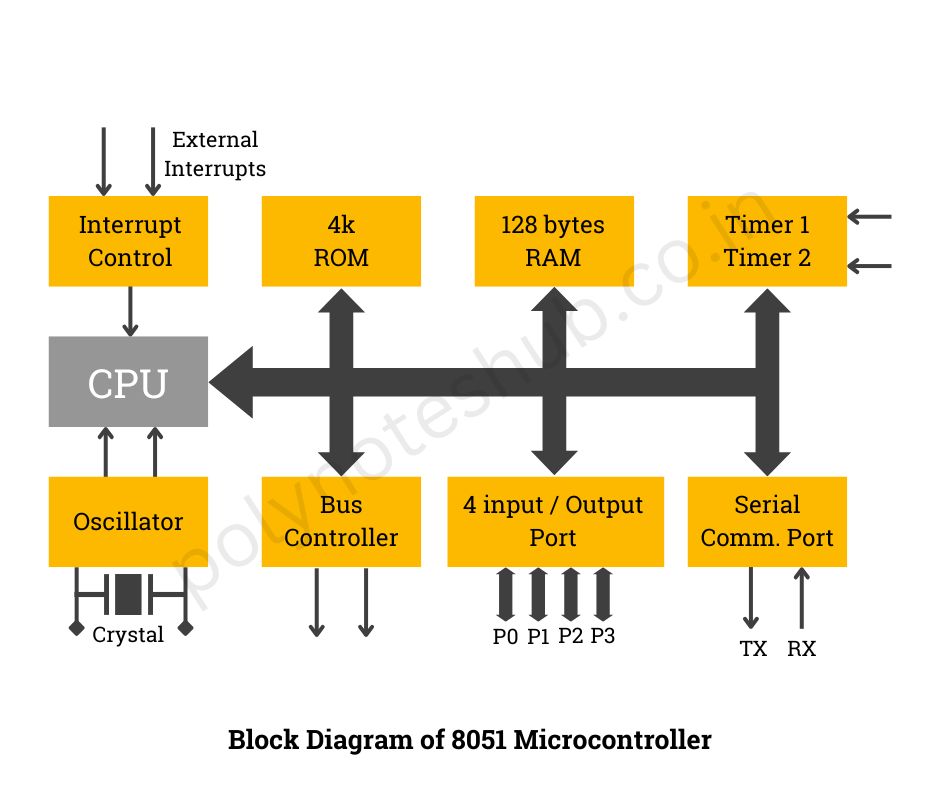
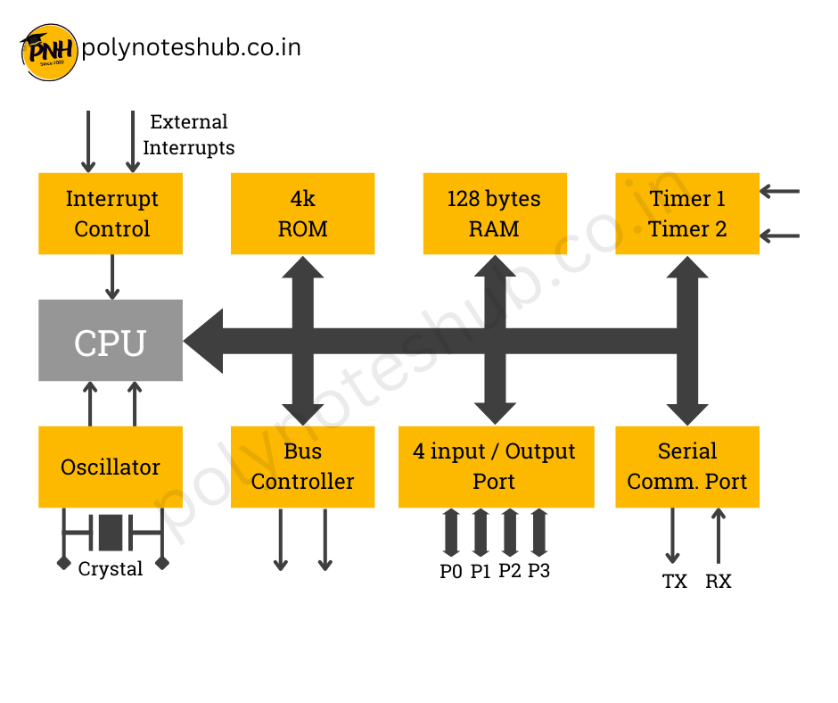
Below we shows the block diagram of 8051 microcontroller. In the block diagram of 8051 microcontroller there are many sections which are the essential part of the 8051 microcontroller. We are discussing each and every section of the block diagram of 8051 microcontroller.

- CPU ( Central Processing Unit ): As we know that the CPU is the brain of any processing device of the microcontroller. It monitors and controls all operations that are performed on the Microcontroller units. The user has no control over the work of the CPU directly. It reads a program written in ROM memory and executes them and does the expected task of that application. In the block diagram of 8051, the CPU is the most essential part.
- Interrupts: As its name suggests, Interrupt is a subroutine call that interrupts the Microcontrollers main operations or work and causes it to execute any other program, which is more important at the time of operation. The feature of interrupt is very useful as it helps in case of emergency operation. Generally 5 interrupt sources are there in 8051 Microcontroller. There are 5 vectored interrupts are shown in below:
- INT0
- INT1
- TF0
- TF1
- R1/T1
- Memory: The 8051 Microcontroller requires memory on which these can be saved and read by the Microcontroller to perform the specific operation of a popular task. The memory which is used to store the program is known as Code Memory or Program Memory. It is known as ROM. For temporary storage, another kind of memory is used which is called RAM. 8051 Microcontroller has 4k of code memory and 128 bytes of RAM.
- BUS: Basically, BUS is collection of wires which work as a communication channel or medium for transfer the data. These buses consists of 8, 16 or more wires of the microcontroller. Thus, these can carry 8 bits simultaneously. Here two types of Buses that are shown below:
- Address Bus: In the block diagram of 8051 microcontroller has a 16 bit address bus for transferring the data. It is used to address memory locations and to transfer the address from CPU to Memory of the Microcontroller.
- Data Bus: In the block diagram of 8051 microcontroller has 8 bits of the data bus, which is used to carry data of particular applications.
- Oscillator: Generally, we know that the microcontroller is a device, therefore it requires clock pulses for its operation of microcontroller applications. For this purpose, 8051 has an Chip oscillator which is a clock source for the Central Processing Unit of the microcontroller. The output pulses of the oscillator are stable. Therefore, it enables the synchronized work of all parts of the 8051 microcontroller.
- Input/Output Ports: Normally, Microcontroller is used in Embedded systems to control the operation of machines in the microcontroller. Therefore, to connect it to other machines, devices, or peripherals we require I/O ports in the microcontroller interface. For this purpose, the block diagram of 8051 has 4 input, and output ports to connect it to the other peripherals.
- Timers/ Counters: Block diagram of 8051 microcontroller has two 16 bits timers and counters. These counters are again divided into an 8-bit register. The timers are used for the measurement of intervals to determine the pulse width of the pulse.
To summarize, the 8051 microcontroller remains a cornerstone in the field of embedded systems due to its simplicity, adaptability, and broad range of applications. It is a popular choice for both beginners and professionals due to its sturdy architecture and ability to execute a wide range of activities. The Block Diagram of 8051 Microcontroller is a crucial tool for understanding its internal components and relationships, making system design and implementation easier.
Analyzing the Block Diagram of 8051 Microcontroller reveals the smooth integration of components such as memory, timers, I/O ports, and serial communication, all of which are crucial in real-world applications. For anyone new to microcontroller programming, a thorough examination of the block diagram of 8051 microcontroller gives a solid basis for learning this versatile technology.

