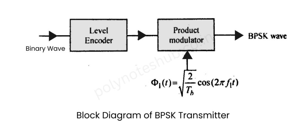
In this note, we are going to learn about the Block Diagram of BPSK Transmitter and Receiver. Welcome to Poly Notes Hub, a leading destination for engineering notes for diploma and degree engineering students.
Author Name: Arun Paul.
What is the BPSK Modulation Technique?
BPSK Modulation (Binary Phase Shift Keying) is a basic and widely used digital modulation technique. It is a form of Phase Shift Keying (PSK) that uses two unique phase states (often 0° and 180°) to encode binary digits:
- Bit 0 → phase 0°
- Bit 1 → phase 180°
This means that the carrier signal’s phase is changed according to the digital data signal, transmitting one bit per symbol.
Advantages of BPSK Modulation
- Easy to design and implemented.
- Use low power comparing to other modulation technique.
- This technique is ideal for low data rate and long distance communication as well.
Disadvantages of BPSK Modulation
- It is not suitable for high speed communication.
- It has poor spectral efficiency compared to QPSK.
- It needs complex receiver circuit to do coherent detection.
Block Diagram of BPSK Transmitter and Receiver
Here we have discussed both the block diagrams of BPSK transmitter and receiver. The generation of BPSK is done in the transmitter section, and the detection of BPSK is done by the receiver section.
Block Diagram of BPSK Transmitter (Generation of BPSK)
The BPSK transmitter comprises a level encoder and a product modulator. The transmitter receives a binary wave consisting of a stream of bits (0s and 1s). The level encoder turns these binary bits into bipolar signals, with ‘1’ represented as +1 and ‘0’ as -1. This conversion is required for phase modulation. The encoded signal is then supplied to the product modulator. The product modulator multiplies the encoded binary signal with a high-frequency carrier signal ϕ1(t). The equation of the ϕ1(t) is given in the picture below.

Depending on whether the bit is +1 or -1, the phase of the carrier maintains 0° or moves to 180°, resulting in the BPSK waveform. The resulting signal is BPSK modulated, with each bit encoded by a phase change. This BPSK wave is subsequently sent along the communication channel to the receiver.
Block Diagram of BPSK Receiver (Detection of BPSK)
The BPSK receiver attempts to recover the original binary data from the received BPSK signal. The first block is a multiplier, which multiplies the incoming BPSK signal with a locally generated carrier signal that is identical to the one used by the transmitter. This multiplication aids in transforming the signal to baseband. The result is then fed to an integrator, which integrates the signal over a one-bit time, filtering out noise and obtaining the appropriate signal component.

Then the integrator produces a voltage level that is either positive or negative, depending on whether the received phase was 0° or 180°. This signal goes into a decision-making device, which compares the output to a predefined threshold (typically zero). If the value is larger than zero, it is detected as bit ‘1’; otherwise, it is detected as bit ‘0’. Thus, the original binary data is retrieved.

