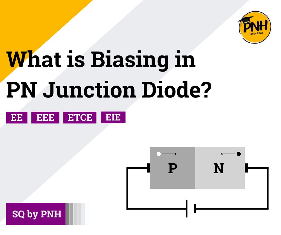
In this blog, we are going to know this topic called “What is Biasing in PN Junction Diode?” Welcome to Poly Notes Hub, a leading destination for engineering notes for diploma and degree engineering students.
Author Name: Arun Paul
Introduction
A PN junction diode is one of the most fundamental components in electronics. Biasing in a PN junction diode is a process that involves applying a voltage across the diode to control its operation. This concept is essential for understanding how diodes function in different circuits, including rectifiers, amplifiers, and switches. Let us explore what biasing is in a PN junction diode and how it works under different conditions.
What is Biasing in PN Junction Diode?
Biasing refers to applying a specific voltage to a PN junction diode to determine its state of operation. The state can either be forward-biased or reverse-biased, depending on how the voltage is applied. This simple yet crucial concept plays a significant role in modern electronics.
Types of Biasing in PN Junction Diode
- Forward Biasing: Forward biasing occurs when the positive terminal of a power source is connected to the P-side (anode) and the negative terminal to the N-side (cathode). This reduces the potential barrier, allowing current to flow through the diode. Learn more about PN junction operation and the concept of electrical conduction.
- Reverse Biasing: In reverse biasing, the positive terminal is connected to the N-side, and the negative terminal is connected to the P-side. This increases the potential barrier, preventing current flow. Only a small leakage current flows due to minority carriers. Check out details on reverse bias and leakage current.
Why Biasing is Important
Biasing in a PN junction diode is critical for controlling the flow of current and voltage in electronic circuits. Whether it’s for rectification, signal modulation, or voltage regulation, biasing helps achieve the desired operation of the diode.
Working of a Biased PN Junction Diode
- Forward Bias Characteristics: When the diode is forward-biased, the depletion region narrows, and charge carriers flow across the junction. The forward-biased diode exhibits a low resistance, enabling current flow. Learn more about forward conduction.
- Reverse Bias Characteristics: Under reverse bias, the depletion region widens, and the diode offers high resistance. This characteristic is useful for applications like clipping circuits and clamping circuits.
Applications of Biasing in PN Junction Diode
Biasing in PN junction diode is used in:
- Rectifiers for converting AC to DC.
- Clipping and Clamping Circuits to shape signals.
- Voltage Regulation in power supplies.
For engineering students, mastering these applications is vital. Explore more such topics on Poly Notes Hub.
Conclusion
Understanding what biasing is in a PN junction diode is crucial for building a strong foundation in electronics. Whether it’s forward or reverse biasing, each type plays a unique role in determining the diode’s operation. For more in-depth engineering notes and guides, visit Poly Notes Hub today.
For additional reading, check out resources on semiconductor diodes, depletion regions, and semiconductor basics.

