What is Microprocessor?
Microprocessor is a controlling unit of a microcomputer, fabricated on a small chip capable of performing ALU (Arithmetic Logical Unit) operations and communicating with the other devices connected to it.
The microprocessor consists of an ALU, a register Array, and a Control Unit.
ALU performs arithmetical and logical operations on the data received from the memory or an input device. Register array consists of registers identified by letters like B,C,D,E,H,L and Accumulator. The control unit control the flow of data and instructions within the computer.
Block diagram of a Basic Microcomputer

How does a Microprocessor work?
Initially, the instructions are stored in the memory in sequential order. The microprocessor fetches those instructions from the memory, then decodes them and executes those instructions till the STOP instruction is reached. Later, it sends the result in binary to the output port. Between these processes, the register stores the temporary data and ALU performs the computing functions.
List of terms that are used in a Microprocessor-
- Instruction Set: It is the set of instructions that the microprocessor can understand.
- Bandwidth: It is the no of bits processed in a single instruction.
- Clock Speed: It determines the no of operations per second the processor can perform.
- Word Length: It depends upon the width of the internal data bus, registers, ALU, etc. An 8-bit microprocessor can process 8-bit data at a time. The word length ranges from 4-bit to 64-bit depending upon the type of the microcomputer.
- Data Types: The microprocessor has multiple data type formats like binary, BCD, ASCII, and signed and unsigned numbers.
Features of a Microprocessor
- Cost-effective: These are available at low prices.
- Size: These are small in size.
- Low Power Consumption: These are made by using MOSFET which is low power consumption.
- Reliability: The failure rate is very low.
About 8085 Microprocessor
The 8085 Microprocessor is an 8-bit microprocessor introduced by Intel in 1976. It is a central processing unit (CPU) designed to perform various computing tasks and control functions within electronic devices. The “8-bit” designation refers to the width of the data bus, which means the microprocessor can process 8 bits of data at a time.
The 8085 Microprocessor became widely used in various applications, including early personal computers, industrial automation, embedded systems, and educational purposes. It played a significant role in the development of computing technology, particularly during the late 1970s and early 1980s.
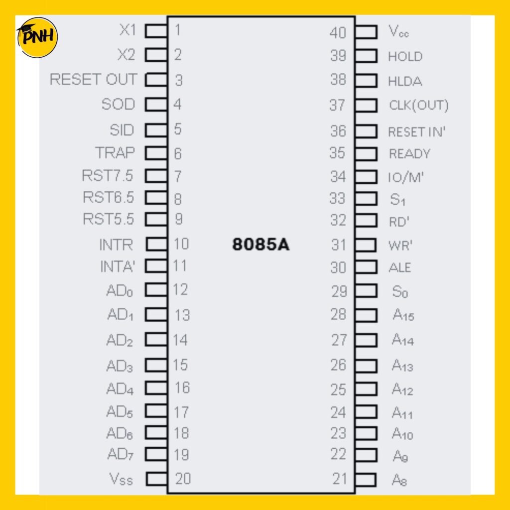
Pin Diagram of 8085 Microprocessor

Here is a brief explanation of the pin diagram:
- VCC (+5V): This pin provides the supply voltage to the microprocessor. It requires a regulated +5V DC power supply for proper operation.
- GND (Ground): Connected to the ground, this pin serves as the reference voltage for the microprocessor’s operation.
- INTR (Interrupt Request): External devices can use this pin to send interrupt requests to the microprocessor.
- RST 7.5 (Restart 7.5): This is one of the restart pins used to reset the microprocessor. It is a non-maskable interrupt and has the highest priority.
- RST 6.5 (Restart 6.5): Another restart pin with lower priority than RST 7.5.
- RST 5.5 (Restart 5.5): The third restart pin with even lower priority.
- TRAP: This is the trap interrupt pin, which is used for non-maskable interrupt requests.
- RST 5.5: The fourth restart pin with even lower priority.
- SID (Serial Input Data): Used for serial data input to the microprocessor.
- SOD (Serial Output Data): Used for serial data output from the microprocessor.
- IO/M (Input/Output and Machine Cycle): This pin distinguishes between memory and I/O operations during machine cycles.
- HLDA (Hold Acknowledge): Indicates that the microprocessor has received the HOLD request and is relinquishing control of the buses.
- ALE (Address Latch Enable): Generates a signal to latch the address from the address bus during the first clock cycle of a machine cycle.
- AD0-AD7 (Address/Data Bus): These lines carry both address and data information during various machine cycles.
- A15-A8 (Higher Order Address Bus): These lines carry the higher-order address bits during memory and I/O operations.
- S1 and S0 (Status): These pins indicate the status of the microprocessor during various operations.
- WR (Write): This signal indicates a write operation from the microprocessor to an external device.
- RD (Read): This signal indicates a read operation from an external device to the microprocessor.
- READY: Indicates that the external device is ready to communicate with the microprocessor.
- ALE (Address Latch Enable): Same as pin 13.
- INTA (Interrupt Acknowledge): This signal indicates that the microprocessor has acknowledged an interrupt request.
- RESET IN: This is the external reset input used to reset the microprocessor.
- X1 and X2 (Crystal Oscillator Pins): These pins are connected to an external crystal oscillator that provides the clock signal for the microprocessor.
- CLK (Clock): Provides the system clock input to the microprocessor.
- RESET OUT: This is the reset output signal generated by the microprocessor to reset external devices.
- Hold: This pin is used to pause the microprocessor’s operation temporarily.
- HLDA (Hold Acknowledge): Same as pin 12.
- VSS (Ground): Same as pin 20.
Microprocessor Vs Microcontroller
| Microcontroller | Microprocessor |
|---|---|
| 1. Memory is Inbuilt. | 1. Memory is externally connected. |
| 2. It is used for specific applications. | 2. It is used for general purpose. |
| 3. Microcontroller = CPU + peripheral + memory. | 3. Microprocessor = CPU. |
| 4. Complex and Expensive. | 4. Simple and Affordable. |
| 5. Require more instructions. | 5. Require fewer instructions. |
Posted To:
Show your Love at !
You can check also:
- Architecture of 8051 Microcontroller
- Pin Diagram of 8051 Microcontroller
- About TRIAC
- Triggering Methods of SCR

