In this note, we are going to know about IGBT Transistor or Insulated Gate Bipolar Transistor. About its construction, working, specifications, characteristics, and applications. Welcome to Poly Notes Hub, a leading destination for engineering notes for diploma and degree engineering students.
Author Name: Arun Paul.
What is IGBT Transistor?
The Insulated Gate Bipolar Transistor (IGBT) is a semiconductor device that combines MOSFETs’ high-speed switching performance with BJTs‘ or Bipolar Junction Transistor high voltage and current handling capabilities. It is frequently utilized in power electronics applications.
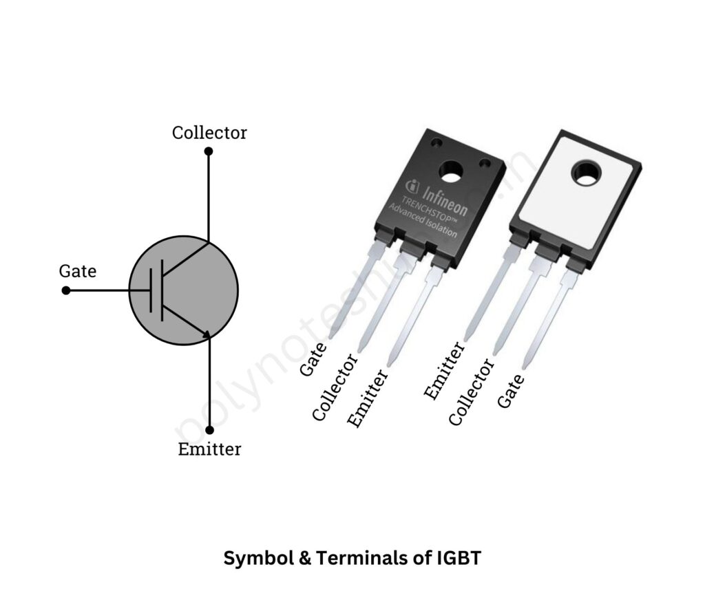
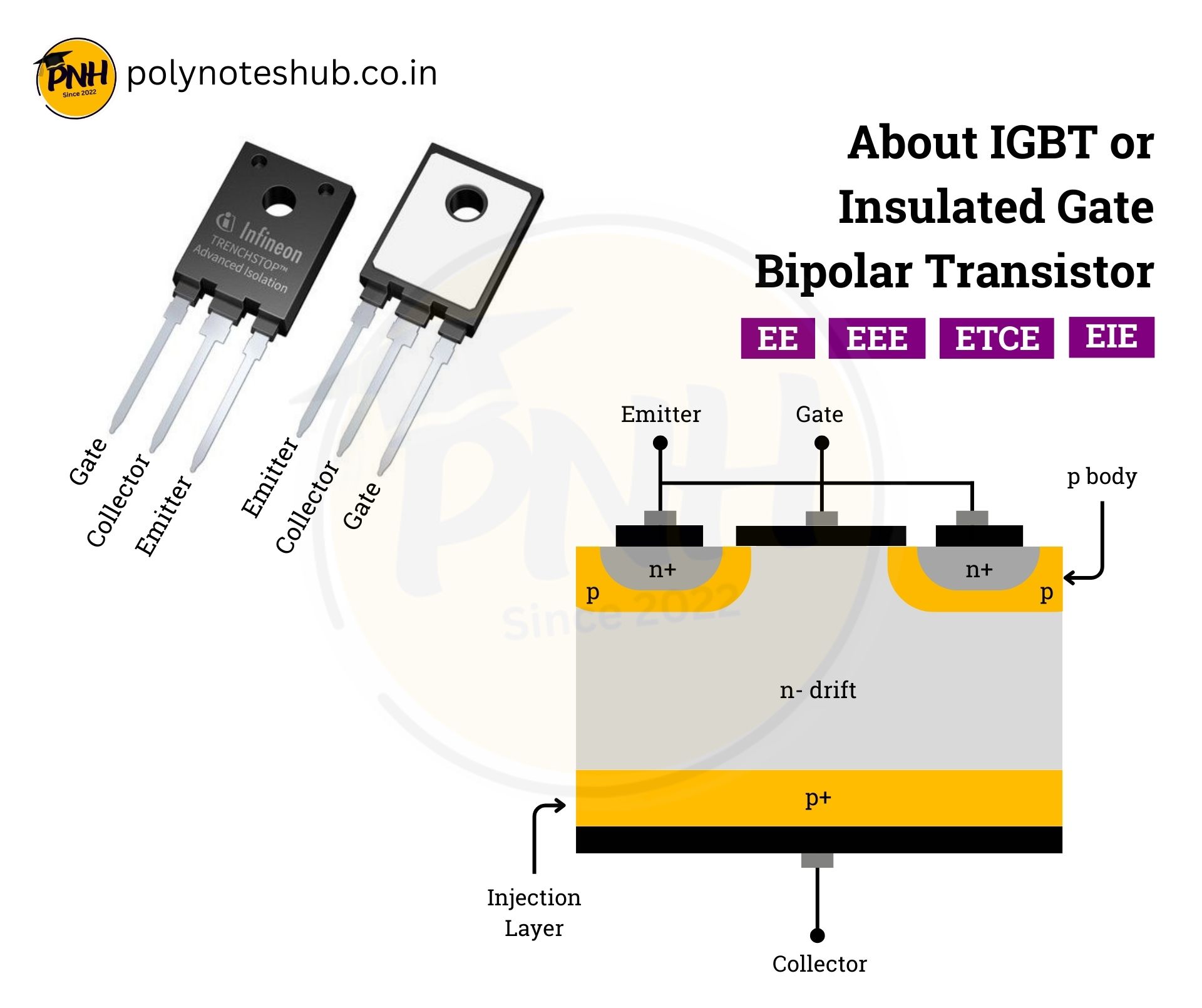
Terminals of IGBT or Insulated Gate Bipolar Transistor
- Gate (G) – This terminal controls the switching operation by applying a voltage.
- Emitter (E) – This terminal acts as the main input terminal where the current enters.
- Collector (C) – The output terminal where current exits the device.

Key Characteristics of Insulated Gate Bipolar Transistor or IGBT
- It has high speed switching like a MOSFET.
- It has high current and voltage handling like a Bipolar Junction Transistor.
- It is a voltage controlled device used mainly in power electronics applications.
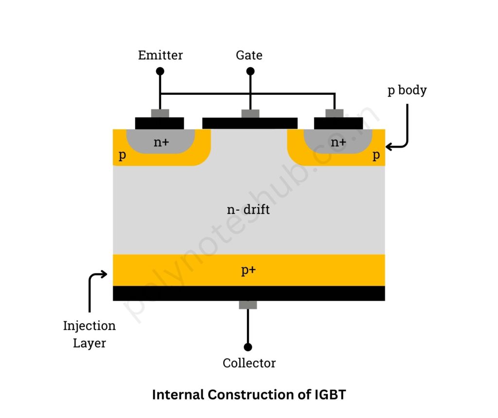
Internal Structure or Construction of IGBT Transistor

The IGBT is built using the following layers –
- P+ Substrate (Collector Region):
- This is the bottom layer of the IGBT.
- It is responsible for injecting holes into the drift region.
- This helps in reducing conduction losses, making the IGBT more efficient.
- N- Drift Region:
- This is the thickest layer and determines the voltage blocking capability of the IGBT.
- It acts as the base for the internal BJT structure.
- P- Body Region:
- This region forms the junction with the N drift layer and prevents latch-up issues.
- It ensures the IGBT functions like a controlled switch.
- N+ Emitter Region (Emitter Contact):
- This region allows electrons to enter into the drift region.
- It forms the emitter of the internal BJT.
Operation of IGBT Transistor
IGBT works as a voltage controlled device, where a small gate voltage controls a large current flow between the collector and emitter.
It operates in three main regions –
- OFF State: When no gate voltage (VGS) is applied, the device remains non-conducting.
- ON State: When a positive gate emitter voltage (VGE > Vthreshold) is applied, the MOSFET inside the IGBT turns ON, allowing current to flow through the device.
- Saturation Region: The IGBT conducts fully, minimizing power loss.
Advantages of IGBT
Here are the advantages of Insulated Gate Bipolar Transistor –
- It is high efficient transistor.
- It can handle up to >1 kV in industrial applications.
- It has fast switching speed.
- This transistor reduces power consumption.
Disadvantages of IGBT
Here are the disadvantages of Insulated Gate Bipolar Transistor –
- It has more switching losses.
- If excessive current flows, it may lead to permanent damage.
Applications of IGBT
Here are the applications of Insulated Gate Bipolar Transistor –
- Used in UPS, solar inverters, and motor drives.
- Employed in motor controllers and battery management.
- Used in industrial heating applications.
- For high voltage power transmission lines.
- Used in electric locomotives and metro trains.


