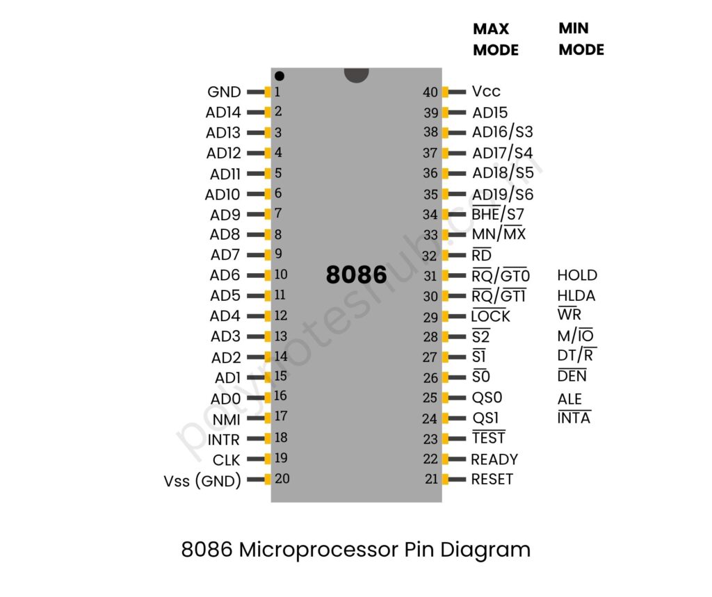
In this note, we are going to know about the 8086 Microprocessor pin diagram with explanation. We are explaining the function of each pin of this microprocessor. Welcome to Poly Notes Hub, a leading destination for polytechnic or diploma engineering notes for polytechnic students.
Author Name: Arun Paul.
8086 Microprocessor Pin Diagram with Explanation
About 8086 Microprocessor
The 8086 microprocessor is a 16-bit microprocessor invented by Intel in 1978. It has a 20-bit address bus and can access 1 MB of memory. It works in minimum and maximum modes, provides pipelining via a 6-byte instruction queue, and serves as the foundation for the x86 processor family found in most current computers.
Key Features of 8086 Microprocessor
- 16-bit ALU (Arithmetic Logic Unit)
- 20-bit Address Bus
- 16-bit Data Bus
- Segmented Memory Architecture
- 6-byte Prefetch Queue (Pipelining)
- Two Operating Modes
- 40 Pins Total
Here is the pin diagram of the 8086 microprocessor with the function of each pin –

1. Address/Data Bus
| Pin(s) | Name | Description |
|---|---|---|
| AD0–AD15 | Address/Data Bus | These are multiplexed lines. During the first part of the bus cycle, they carry the address, and during the second part, they carry data. |
| A16–A19/S3–S6 | Address/Status Bus | These are multiplexed lines used to provide the upper 4 bits of the 20-bit address or status signals depending on the cycle. |
2. Control and Status Signals
| Pin | Name | Description |
|---|---|---|
| M/IO | Memory/Input Output | Tells whether the current operation is memory access (1) or I/O operation (0). |
| RD | Read | Signals that the microprocessor is performing a read operation. |
| WR | Write | Signals that the microprocessor is performing a write operation. |
| DT/R | Data Transmit/Receive | Used to control the direction of data flow through transceivers. |
| DEN | Data Enable | Enables the transceivers (data buffers). |
| ALE | Address Latch Enable | Indicates that valid address is available on the multiplexed bus. It helps to latch the address. |
| INTA | Interrupt Acknowledge | Indicates the processor has acknowledged an interrupt request. |
| TEST | Test | Used to synchronize with external WAIT signals during debugging. |
3. Interrupt and DMA (Direct Memory Access) Pins
| Pin | Name | Description |
|---|---|---|
| INTR | Interrupt Request | General-purpose interrupt line. Activated by an external device. |
| NMI | Non-Maskable Interrupt | Cannot be disabled by software; used for emergency or high-priority interrupts. |
| HOLD | Hold | Indicates that another device is requesting the use of the address/data bus. |
| HLDA | Hold Acknowledge | Indicates that the processor has granted the bus control to another device. |
4. Clock and Power Pins
| Pin | Name | Description |
|---|---|---|
| CLK | Clock | Provides timing for synchronization of internal operations. |
| RESET | Reset | Initializes the microprocessor and starts execution from memory location FFFF0H. |
| VCC | Power Supply | +5V DC power supply. |
| GND | Ground | 0V reference for the power supply. |
5. Ready and Queue Status
| Pin | Name | Description |
|---|---|---|
| READY | Ready | Used to insert wait states for slow memory or I/O devices. |
| QS0, QS1 | Queue Status | Indicate the status of the instruction queue (used in pipelining). |


