
For engineering students and beginners, understanding PCB manufacturing is an important step toward learning how electronic products are designed and produced. This guide explains the complete PCB manufacturing process, the major materials used, different types of PCBs, and how PCB fabrication differs from PCB assembly.
Printed Circuit Boards (PCBs) are one of the most important components in modern electronic devices. From smartphones and computers to industrial machines, medical equipment, automobiles, and communication systems, PCBs provide the physical and electrical foundation required to connect electronic components.
Author Name: Arun Paul.
What Is PCB Manufacturing?
PCB manufacturing is the process of producing a printed circuit board from a circuit design. It involves creating conductive copper pathways on an insulating substrate so that electronic components can communicate electrically when mounted on the board.
A PCB typically consists of several layers, including:
- Substrate material
- Copper layers
- Solder mask
- Silkscreen
- Surface finish
The complexity of the manufacturing process depends on the type of PCB, number of layers, required tolerances, materials, and intended application.
Why Is PCB Manufacturing Important?
PCBs make it possible to build compact, reliable, and organized electronic circuits. Instead of connecting components using individual wires, a PCB uses carefully designed copper traces to create electrical connections.
Some major advantages of PCB-based electronics include:
- Compact design: Components and connections can be arranged efficiently.
- Reliability: Properly manufactured boards provide stable electrical connections.
- Repeatability: The same PCB design can be manufactured multiple times.
- Easy assembly: Automated processes can place large numbers of components accurately.
- Better organization: Electrical connections are integrated directly into the board.
For engineering students, understanding these advantages helps connect theoretical electronics concepts with real-world manufacturing.
Main Materials Used in PCB Manufacturing
Different materials are used depending on the application and performance requirements.
1. Substrate
The substrate provides the mechanical foundation of the PCB. FR-4, a glass-reinforced epoxy laminate, is one of the most commonly used materials for general-purpose PCBs. Other materials may be selected for applications requiring specific thermal, electrical, mechanical, or flexibility characteristics.
2. Copper
Copper forms the conductive pathways that connect different components. Copper layers can be present on one or both sides of a simple PCB, while multilayer boards contain multiple copper layers separated by insulating material.
3. Solder Mask
The solder mask is the protective coating usually applied over the copper circuitry. It helps protect traces from contamination and reduces the risk of unintended solder connections during assembly.
4. Silkscreen
The silkscreen layer contains printed information such as component references, labels, logos, and polarity indicators. It helps engineers and technicians identify components during assembly and testing.
5. Surface Finish
A surface finish is applied to exposed copper areas, particularly component pads. Different surface finishes can be selected depending on manufacturing requirements, component compatibility, durability, and cost.
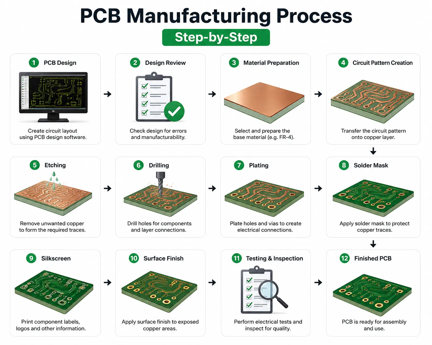
PCB Manufacturing Steps or Process: Step-by-Step
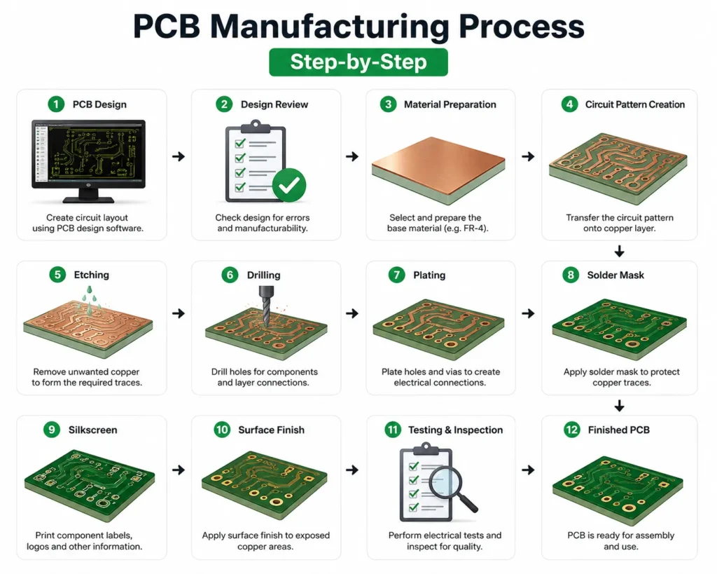
The PCB manufacturing process consists of several stages. Although the exact workflow varies depending on the board design and manufacturer, the following steps represent a typical PCB production process.
Step 1: PCB Design
PCB manufacturing begins with a digital PCB design.
Engineers use PCB design software to create:
- Schematic diagrams
- Component footprints
- Copper traces
- Board outlines
- Vias
- Layer arrangements
The design must be checked carefully before manufacturing because design errors can result in electrical or mechanical problems.
Step 2: Design Review and Preparation
Before fabrication begins, the design is reviewed to identify potential manufacturing problems.
This stage may include checking:
- Trace width
- Spacing
- Hole sizes
- Component placement
- Layer alignment
- Manufacturing tolerances
A manufacturer may also perform a Design for Manufacturing (DFM) review to determine whether the design can be produced reliably.
Step 3: Material Preparation
The appropriate substrate and copper-clad material are selected according to the board specifications. For example, a standard rigid PCB may use an FR-4 substrate, while specialized applications may require different materials.
Step 4: Creating the Circuit Pattern
The required circuit pattern is transferred onto the copper surface. Depending on the manufacturing technology, imaging and etching processes are used to create the desired conductive traces. Unwanted copper is removed while the required copper pattern remains.
Step 5: Layer Formation
For multilayer PCBs, multiple conductive and insulating layers are combined. Each layer must be aligned accurately because even small alignment errors can affect electrical connections. Multilayer construction allows manufacturers to create more complex circuits while keeping the overall board size relatively compact.
Step 6: Drilling
Holes are created in the PCB for component mounting and electrical connections between layers.
Depending on the design, these can include:
- Through-holes
- Vias
- Blind vias
- Buried vias
Modern PCB manufacturing can use highly precise mechanical or laser drilling technologies depending on the board requirements.
Step 7: Plating
Plating processes are used to create conductive connections between appropriate copper layers and to provide the required copper thickness in holes and other areas. This is particularly important for multilayer boards where electrical connections must pass between different layers.
Step 8: Applying the Solder Mask
The solder mask is applied to protect the copper traces and leave only the required soldering areas exposed. This layer also gives the PCB its familiar appearance and helps prevent accidental solder bridges during PCB assembly.
Step 9: Silkscreen Printing
Information such as component identifiers, logos, warnings, and polarity markings can be printed on the board. This makes component placement and inspection easier.
Step 10: Surface Finishing
Exposed copper pads receive an appropriate surface finish. The choice depends on factors such as component type, board requirements, manufacturing volume, reliability requirements, and cost.
Step 11: Electrical and Visual Testing
Before a finished PCB is shipped, manufacturers may perform different inspections and tests.
These can include:
- Visual inspection
- Automated optical inspection (AOI)
- Electrical testing
- Dimensional inspection
- Other quality-control procedures
The objective is to identify manufacturing defects before the board reaches the assembly or final-product stage.
PCB Fabrication vs PCB Assembly
Beginners often confuse PCB fabrication with PCB assembly, but they are different processes.
PCB Fabrication
PCB fabrication creates the physical bare board.
It includes processes such as:
Layer formation → imaging → etching → drilling → plating → solder mask → surface finish
PCB Assembly
PCB assembly involves mounting electronic components onto the finished PCB.
Components may include:
- Resistors
- Capacitors
- Diodes
- Transistors
- Integrated circuits
- Connectors
- Relays
Two common assembly technologies are Surface Mount Technology (SMT) and Through-Hole Technology (THT).
Therefore:
PCB Manufacturing = Fabrication + related board production processes
PCB Assembly = Mounting electronic components onto the fabricated PCB
The exact terminology can vary between manufacturers and industry contexts, so students should always check how a particular supplier defines its services.
Types of PCBs
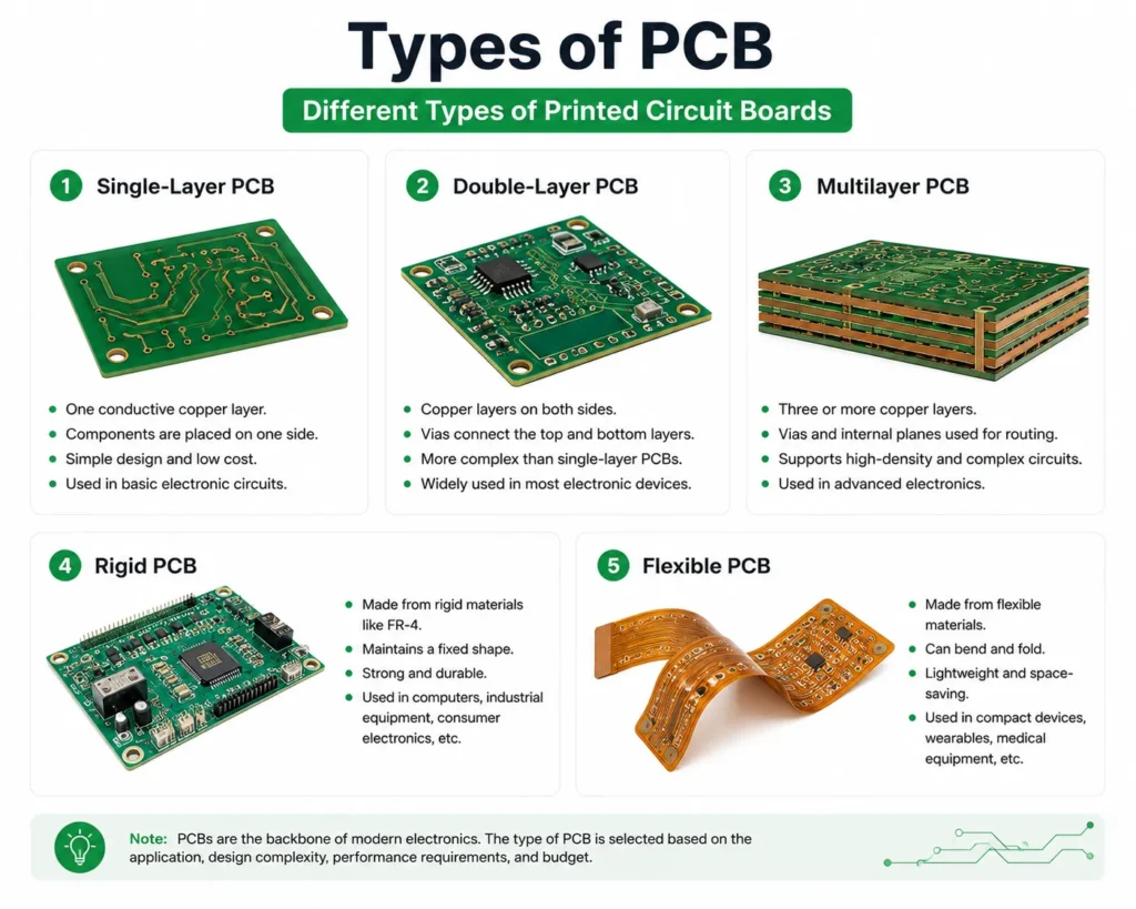
PCBs can be classified in several ways.
- Single-Layer PCB: A single-layer PCB contains one primary conductive copper layer. These boards are generally suitable for relatively simple circuits.
- Double-Layer PCB: A double-layer PCB has conductive copper layers on both sides of the substrate. Vias can connect electrical paths between the layers.
- Multilayer PCB: Multilayer PCBs contain multiple conductive layers separated by insulating materials. They are widely used when circuits require greater density and complexity.
- Rigid PCB: Rigid PCBs maintain a fixed shape and are widely used in computers, industrial electronics, consumer devices, and many other products.
- Flexible PCB: Flexible PCBs can bend and conform to different shapes. They are useful where space, weight, or mechanical movement is important.
Factors to Consider When Choosing a PCB Manufacturer
When a company needs a PCB, choosing a suitable PCB manufacturer involves more than comparing prices.
Important factors include:
- Manufacturing Capability: Check whether the manufacturer can produce the required board type, layer count, dimensions, materials, and tolerances.
- Quality Control: Reliable inspection and testing procedures are important for maintaining consistent PCB quality.
- Production Capacity: A supplier suitable for prototypes may not necessarily be the best option for high-volume production.
- Lead Time: Production schedules can be important for both prototype development and commercial manufacturing.
- Cost: PCB cost can depend on:
- Board size
- Number of layers
- Material
- Copper thickness
- Quantity
- Surface finish
- Hole requirements
- Manufacturing complexity
- Technical Support: Good technical communication can help identify manufacturing issues before production begins.
Common PCB Manufacturing Problems
Some common manufacturing problems include:
- Incorrect dimensions
- Poor layer alignment
- Inadequate copper thickness
- Drilling defects
- Solder mask problems
- Surface finish issues
- Electrical connectivity failures
- Manufacturing contamination
Proper design review, DFM analysis, process control, inspection, and testing can help reduce these problems.
PCB Manufacturing for Engineering Students
For engineering students, learning about PCB manufacturing provides a practical connection between classroom concepts and real-world electronics.
Students studying Electrical Engineering, Electronics Engineering, Electronics and Telecommunication Engineering, Instrumentation Engineering, and related disciplines can benefit from understanding:
- Circuit design
- PCB layout
- Electronic components
- Manufacturing processes
- Soldering and assembly
- Testing and troubleshooting
- Design for manufacturing
A student who understands the complete journey from circuit schematic → PCB layout → fabrication → assembly → testing has a much clearer understanding of how an electronic product is developed.
How Can Beginners Learn PCB Manufacturing?
Beginners can start with a simple learning path:
- Step 1: Learn basic electronic components.
- Step 2: Understand circuit diagrams and schematics.
- Step 3: Learn PCB layout fundamentals.
- Step 4: Practice using PCB design software.
- Step 5: Study single-layer and double-layer PCB fabrication.
- Step 6: Learn about SMT and THT assembly.
- Step 7: Understand PCB inspection and testing.
- Step 8: Build and test simple PCB projects.
This approach allows beginners to gradually move from theoretical knowledge to practical PCB development.
Conclusion
PCB manufacturing is a multi-stage process that transforms an electronic circuit design into a physical printed circuit board. It involves material selection, circuit pattern creation, drilling, plating, layer formation, solder mask application, surface finishing, and quality testing.
For engineering students and beginners, understanding the PCB manufacturing process is valuable because it connects electronics theory with practical product development. As electronic devices become more compact and sophisticated, knowledge of PCB design, fabrication, assembly, and testing is increasingly useful across many engineering fields.
Whether you are learning electronics for the first time or preparing to work on professional engineering projects, understanding how a PCB is manufactured gives you a strong foundation for exploring modern electronics and manufacturing.