
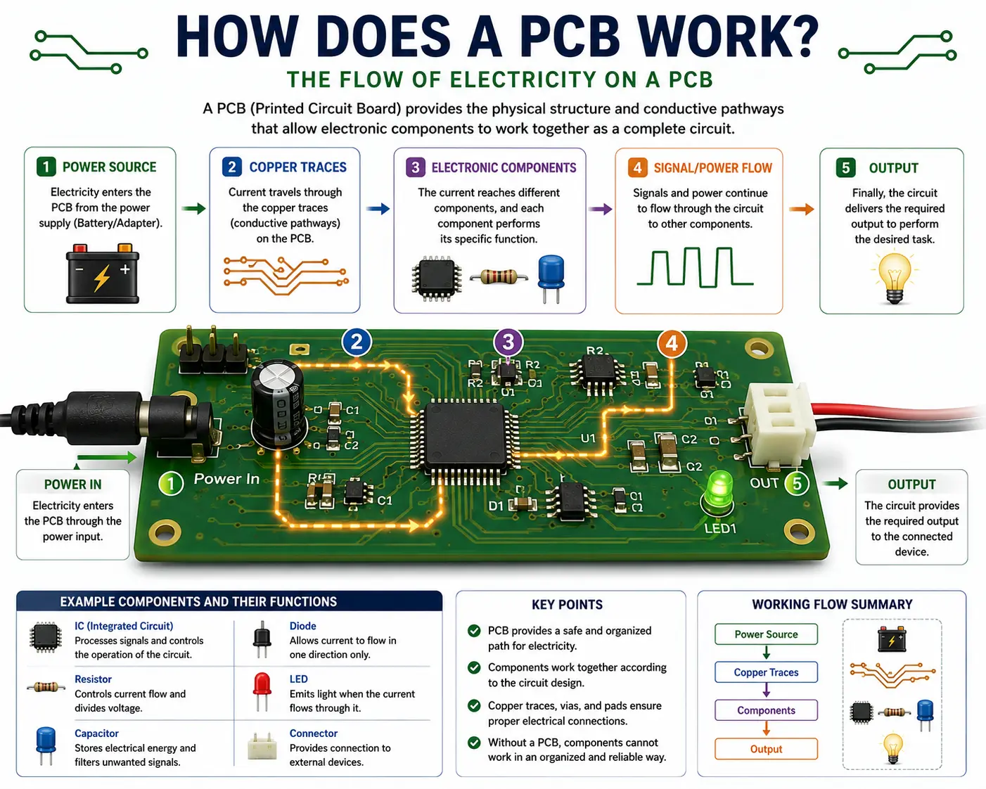
In this guide, we will explain how does a PCB works, its main components and layers, and the basic PCB manufacturing process in a simple and beginner-friendly way.
A Printed Circuit Board (PCB) is one of the most important parts of modern electronic devices. From smartphones and computers to industrial machines, automobiles, medical equipment, and consumer electronics, PCBs provide the electrical connections required for electronic components to work together.
But how does a PCB actually work? What are the different PCB layers and components? And how is a PCB manufactured?
Author Name: Arun Paul.
What Is a PCB?
A Printed Circuit Board (PCB) is a board used to mechanically support and electrically connect electronic components. Instead of connecting components using many individual wires, a PCB uses specially designed conductive pathways called traces.
A standard PCB is made up of an insulating substrate, copper conductive layers, a solder mask, and silkscreen. Resistors, capacitors, integrated circuits (ICs), connectors, and diodes are put on the board and connected by copper traces.
PCBs are available in different designs depending on the application, including single-layer, double-layer, and multilayer PCBs.
How Does a PCB Work?
The basic working principle of a PCB is relatively simple.
When a power source is attached to a PCB, electrical current flows through the copper traces to the relevant electronic components. These components provide a variety of purposes, including voltage control, signal processing, energy storage, circuit switching, and communication with other components.
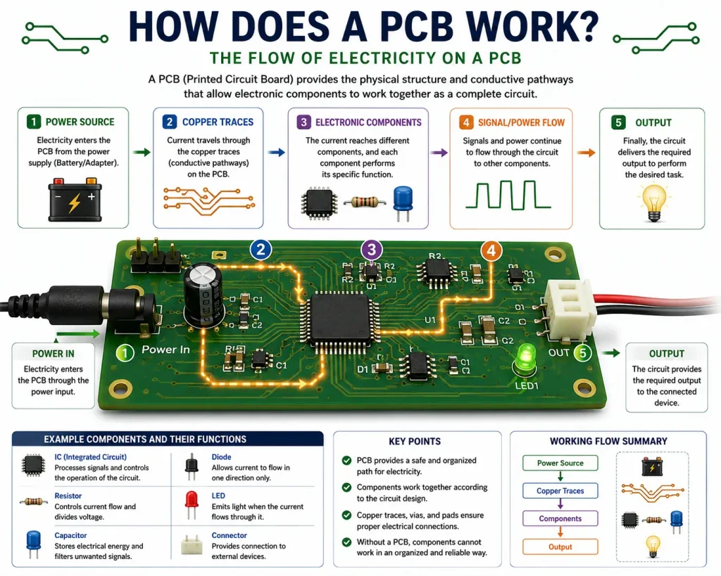
For example, a PCB in an electronic device may contain:
- A power connector for supplying electricity
- Resistors for controlling current and voltage
- Capacitors for filtering and storing electrical energy
- Integrated circuits for processing signals
- Diodes for controlling current direction
- Connectors for connecting external devices
The PCB’s copper traces create predetermined electrical pathways between these components.
As a result, a PCB is rarely used for a single purpose. Instead, it provides the physical structure and electrical connections that make an electronic circuit work.
Main Components of a PCB
Several important components and features work together to create a functional printed circuit board.
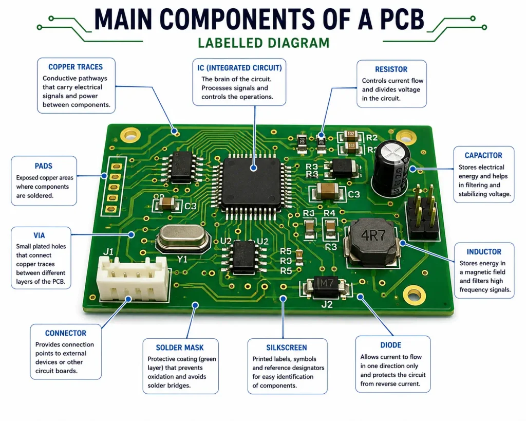
1. Substrate
- The substrate is the basic insulating material of a PCB. It provides mechanical strength and separates conductive paths from each other.
- FR-4, a glass-reinforced epoxy laminate, is one of the most commonly used PCB substrate materials.
2. Copper Traces
- Copper traces are thin conductive pathways created on the PCB. They carry electrical signals and power between different components.
- The width and thickness of a trace can vary depending on the current, voltage, frequency, and design requirements.
3. Pads
- Pads are exposed conductive areas where electronic components are soldered to the PCB.
- Different components require different pad configurations depending on whether they use through-hole or surface-mount technology.
4. Vias
- A via is a small plated hole that provides an electrical connection between different copper layers of a multilayer PCB.
- Vias are especially important in complex PCB designs because they allow signals and power to move between different layers.
5. Solder Mask
- The solder mask is the protective coating commonly seen as the green surface on many PCBs. However, PCBs can also be manufactured with other solder mask colors.
- It helps protect copper traces from oxidation and reduces the possibility of accidental solder bridges during assembly.
6. Silkscreen
- The silkscreen is the printed information on the PCB. It can include component reference numbers, symbols, polarity markings, logos, and other identification information.
Understanding PCB Layers
One of the most important aspects of PCB design is the number of layers.
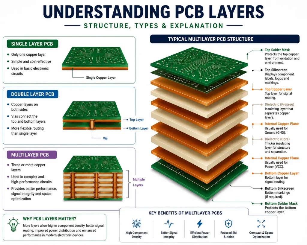
1. Single-Layer PCB
A single-layer PCB contains one conductive copper layer. These PCBs are relatively simple and are commonly used in basic electronic products where circuit complexity is low.
2. Double-Layer PCB
A double-layer PCB has copper layers on both sides of the insulating substrate. Vias can be used to connect circuits between the top and bottom copper layers. Double-sided PCBs provide more routing flexibility than single-layer boards.
3. Multilayer PCB
A multilayer PCB contains three or more conductive layers separated by insulating material. Multilayer PCBs are used for complex electronic devices because they provide greater routing density while allowing designers to create dedicated power and ground planes.
For example, a complex PCB may contain:
- Top signal layer
- Ground plane
- Internal signal layer
- Power plane
- Bottom signal layer
The exact layer structure depends on the requirements of the circuit.
PCB Manufacturing Process
The PCB manufacturing process involves several stages. The exact process can vary depending on the PCB type, material, layer count, and manufacturing requirements.
Step 1: PCB Design
The process starts with designing the circuit using PCB design software.
Engineers create the schematic first and then develop the PCB layout. Component placement, trace routing, board dimensions, vias, and layer configuration are determined during this stage.
Step 2: Preparing the PCB Material
The manufacturer prepares the required substrate and copper materials according to the PCB design specifications.
For multilayer PCBs, multiple copper and insulating layers are prepared for later lamination.
Step 3: Creating the Circuit Pattern
The required circuit pattern is transferred onto the copper surface using specialized manufacturing techniques.
Unwanted copper is removed, leaving the required conductive traces and pads.
Step 4: Drilling
Holes are drilled into the PCB where required.
These holes can be used for through-hole components or vias that electrically connect different PCB layers.
Step 5: Plating
Copper plating is used to create or strengthen electrical connections, particularly inside drilled holes.
This allows electrical signals to travel between the appropriate PCB layers.
Step 6: Applying Solder Mask
A solder mask layer is applied over the PCB surface while leaving the required pads exposed for soldering.
This protects the board and helps prevent unwanted electrical connections during PCB assembly.
Step 7: Applying Silkscreen
Component labels, reference markings, symbols, and other required information can then be printed onto the PCB using the silkscreen process.
Step 8: Surface Finishing
A suitable surface finish is applied to exposed copper areas such as component pads. The finish helps protect the copper and supports reliable soldering.
Step 9: Testing and Inspection
The finished PCB is inspected and tested to identify manufacturing defects and electrical problems.
Depending on the application and manufacturer, different inspection and electrical testing methods may be used.
PCB Assembly vs PCB Manufacturing
It is important to understand that PCB manufacturing and PCB assembly are not exactly the same thing.
PCB manufacturing focuses on producing the bare circuit board, including the substrate, copper traces, vias, solder mask, and other board features.
PCB assembly (PCBA) involves mounting electronic components onto the manufactured PCB. Components can be installed using technologies such as Surface Mount Technology (SMT) and Through-Hole Technology (THT).
After assembly, the completed board can be tested to ensure that the electronic circuit works correctly.
Why Are PCBs Important?
PCBs have become essential because they make electronic circuits more compact, organized, reliable, and scalable.
Some important advantages include:
- Compact circuit design
- Organized electrical connections
- Reduced use of individual wires
- Easier mass production
- Consistent circuit layouts
- Support for complex electronic systems
- Easier maintenance and troubleshooting
Because of these advantages, PCBs are used in almost every major area of modern electronics.
Applications of PCBs
PCBs are found in a wide variety of industries and products, including:
- Smartphones and tablets
- Computers and laptops
- Consumer electronics
- Automotive electronics
- Industrial automation
- Telecommunications equipment
- Medical electronics
- Power electronics
- IoT devices
- Robotics
- Aerospace and defense electronics
The design and manufacturing requirements can vary significantly depending on the application.
Conclusion
Understanding how a PCB works is important for engineering students, electronics enthusiasts, and anyone interested in electronic hardware.
A printed circuit board (PCB) offers the physical structure and conductive pathways necessary for connecting electrical components. Its primary components are the substrate, copper traces, pads, vias, solder mask, and silkscreen. PCBs are classified as single-layer, double-layer, or multilayer boards based on their circuit complexity.
From PCB design and circuit pattern creation to drilling, plating, solder mask application, surface finishing, and testing, PCB manufacturing involves several carefully controlled stages.
As electronics continue to become smaller and more sophisticated, understanding PCB components, PCB layers, PCB manufacturing, and PCB assembly is becoming increasingly valuable for students and professionals in electronics and engineering.